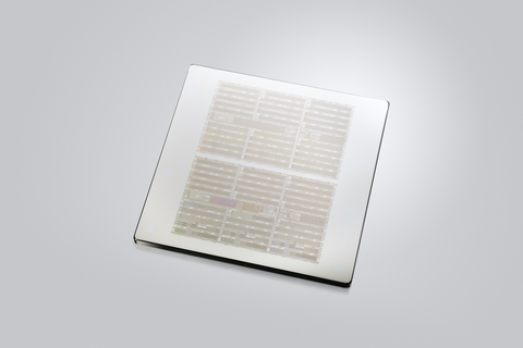
Dai Nippon Printing Co., Ltd. (DNP) announced a breakthrough in semiconductor technology by successfully developing a photomask manufacturing process tailored for the 3-nanometer (3nm) lithography process, specifically supporting Extreme Ultra-Violet (EUV) lithography—a crucial development in semiconductor manufacturing.
DNP has consistently responded to semiconductor manufacturers’ demands for enhanced performance and quality. In 2016, they pioneered the multi-beam mask writing tool (MBMW), drastically reducing lithography time by utilizing approximately 260,000 electron beams. Continuing this trajectory, in 2020, DNP introduced a photomask manufacturing process for 5nm EUV lithography and has since supplied masks meeting the industry’s requirements.
This recent advancement signifies DNP’s focus on further miniaturization in semiconductor manufacturing, developing photomasks for EUV lithography to support 3nm processes. Leveraging the capabilities of the MBMW tool, DNP enhanced the manufacturing process, optimizing data correction technology and processing conditions to cater to the intricate curved pattern structure essential for EUV lithography photomasks.
With plans to operationalize a newly installed MBMW in the latter half of 2024, DNP aims to reinforce its support for advanced semiconductor manufacturing, particularly in the realm of EUV lithography.
Moreover, DNP is poised for collaboration with the Interuniversity Microelectronics Center (imec), an internationally renowned research organization headquartered in Belgium. This collaborative effort aims to jointly develop EUV photomasks for the next generation of EUV exposure equipment.
Looking forward, DNP intends to supply the newly developed 3nm EUV lithography-supporting photomasks to semiconductor manufacturers worldwide. Additionally, the company is committed to advancing peripheral technologies for EUV lithography, targeting an annual sales goal of 10 billion yen by 2030.
Continuing collaborative efforts with partners like imec, DNP aims to push the boundaries of photomask technology, aiming for capabilities that can support processes finer than 3nm and explore advancements beyond the 2nm threshold. This milestone solidifies DNP’s position as a key player in the advancement of semiconductor technology.
