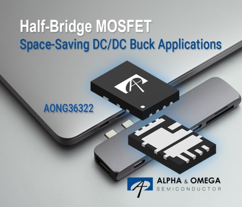
Alpha and Omega Semiconductor Limited (AOS), a leading provider of discrete power devices and modules, has introduced the AONG36322 XSPairFET, catering to the demands of space-constrained DC-DC applications. This innovative MOSFET solution is designed to optimize board space while enhancing power conversion efficiency.
The AONG36322 features two 30V MOSFETs arranged in a half-bridge configuration within an asymmetric DFN3.5×5 XSPairFET package. This design enables a significant reduction in PCB footprint, offering approximately 60 percent space savings compared to conventional solutions. By minimizing space requirements, the AONG36322 streamlines DC-DC architecture, making it ideal for compact applications such as point-of-load (POL) computing, USB hubs, and power banks.
As an extension to the AOS XSPairFET lineup, the AONG36322 incorporates the latest bottom-source packaging technology. It boasts impressive technical specifications, including a maximum on-resistance of 4.5 mOhms for the high-side MOSFET and 1.3 mOhms for the low-side MOSFET at VGS of 10V. Additionally, the direct connection of the low-side MOSFET to the exposed pad on the PCB enhances thermal dissipation, ensuring high performance and reliability in demanding applications.
The AONG36322’s innovative package design effectively reduces parasitic inductance, minimizing switch node ringing and contributing to smoother system operation. This feature enhances the device’s electrical performance, meeting the stringent requirements of modern power electronics applications.
Peter H. Wilson, Marketing Sr. Director of MOSFET product line at AOS, emphasized the AONG36322’s potential to address board space limitations and improve power density and efficiency for developers. With its compact design and advanced features, the AONG36322 enables developers to meet the performance goals of compact applications, driving innovation in power electronics.
The AONG36322 is immediately available in production quantities, with a unit price of $0.915 in 1,000-piece quantities and a lead time of 16 weeks, providing developers with timely access to this advanced MOSFET solution for their DC-DC applications.
