
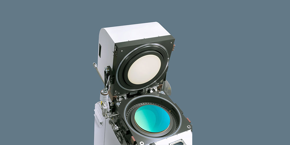
Lam Research Corp. (Nasdaq: LRCX) has introduced a groundbreaking innovation in chip manufacturing with the launch of Coronus DX, the world’s first bevel deposition solution designed to optimize production efficiency and increase chip yield. This cutting-edge solution addresses critical manufacturing challenges in next-generation logic, 3D NAND, and advanced packaging applications.
As the semiconductor industry continues to advance, the complexity of manufacturing processes escalates, requiring hundreds of intricate steps to build nanometer-sized devices on a silicon wafer. Coronus DX revolutionizes chip production by depositing a proprietary protective film on both sides of the wafer edge in a single step. This unique protective layer mitigates defects and potential damage that often occur during advanced semiconductor manufacturing, resulting in higher chip yield and enabling the implementation of new leading-edge processes for the production of next-generation chips.
Sesha Varadarajan, Senior Vice President of the Global Products Group at Lam Research, highlighted the significance of Coronus DX in the current era of chipmaking, stating, “In the era of 3D chipmaking, production is complex and costly. Building on Lam’s expertise in bevel innovation, Coronus DX helps drive more predictable manufacturing and significantly higher yield, paving the way for adoption of advanced logic, packaging, and 3D NAND production processes that weren’t previously feasible.”
Coronus DX complements Lam’s existing Coronus bevel etch technology and acts as a game-changer for chipmakers by facilitating new device structures. During repeated layers of processing, residues and roughness can accumulate along the wafer edge, potentially causing defects and chip failure. Coronus DX effectively resolves these issues by depositing a thin dielectric layer of protection on the bevel. This precise and tunable deposition process addresses common challenges that can impact semiconductor quality, such as material migration and wafer bonding issues in 3D packaging applications, as well as substrate damage in 3D NAND manufacturing caused by long wet etch processes.
Rangesh Raghavan, Corporate Vice President & GM, India at Lam Research, emphasized the importance of collaboration with customers in developing innovative solutions like Coronus DX, stating, “In a complex manufacturing environment, increasing die yield is critical to maximizing fab productivity.”
The introduction of Coronus DX has garnered praise from industry experts. Anne Roule, Head of the Semiconductor Platform Division at CEA-Leti, a research institute in France, said, “CEA-Leti applied its expertise in innovative, sustainable technology solutions to help Lam Research tackle key challenges in advanced semiconductor manufacturing. By simplifying 3D integration, Coronus DX drives significantly higher yield and enables chipmakers to adopt breakthrough production processes.”
The proprietary process behind Coronus DX ensures precise wafer centering and process control, incorporating integrated metrology for consistent and repeatable results. Coronus products incrementally enhance wafer yield, with each etch or deposition step delivering an additional 0.2 to 0.5 percent of yield. Across the wafer flow, this improvement can result in up to a 5 percent increase. Manufacturers running over 100,000 wafer starts per month stand to gain millions of extra die annually, translating to potentially millions of dollars in additional value.
The Coronus product line, initially introduced in 2007, is already widely adopted by every major semiconductor manufacturer, with thousands of chambers installed worldwide. The Coronus and Coronus HP solutions, which employ etch technology to prevent defects by removing layers along the edge, have become industry-leading solutions in bevel technology. These solutions are extensively utilized in the manufacturing of logic, memory, and specialty devices, including state-of-the-art 3D devices. Coronus DX is now being implemented in high-volume manufacturing at leading customer fabs globally.
Hideshi Miyajima (Ph.D.), Technology Executive of Memory Process at Kioxia Corporation, expressed excitement about the collaboration with Lam Research and their Coronus solutions, stating, “Improving quality in the production process through advancements in areas such as bevel technology is essential to our ability to provide next-generation flash memory at scale to our customers. We look forward to continuing to work with Lam Research and its Coronus solutions to enable leading-edge wafer production.”
Lam Research’s introduction of Coronus DX marks a significant milestone in the semiconductor industry, promising increased chip yield, enhanced manufacturing predictability, and the adoption of breakthrough production processes. With its game-changing bevel deposition solution, Lam Research reinforces its position as a leader in bevel technology, supporting chipmakers in their pursuit of cutting-edge chip production.