Silicon Genesis, a pioneering force in semiconductor innovation, has redefined the landscape of CMOS Image Sensor (CIS) fabrication by expanding the application of its NANOCLEAVE Layer Transfer (LT) methods. Originally devised for SOI wafer manufacturing, these methods have now been adapted for 3DIC device stacking, enabling the creation of high-bandwidth CIS devices.
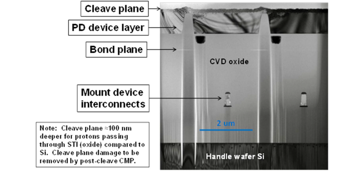
For over a decade, 3D stacking techniques have been instrumental in advanced CIS fabrication, relying on bonding and mechanical grinding die thinning to craft photodiode, memory, and signal output device layers. However, the conventional mechanical grinding methods pose limitations for controlling film thickness in device layers under 20um, inducing internal stresses that lead to issues like recombination leakage currents and heightened refresh cycles for active memory layers. Moreover, these methods result in yield losses due to die edge cracking and constraints on achieving multi-layer stacking at a considerable scale.
Building on their prior success with 3DIC Mega-pixel CMOS BSI Image Sensors, Silicon Genesis is collaborating with partners to extend their NANOCLEAVE process to multiple-layer CIS products, breaking beyond the confines of three and four-layer stacks.
The outcome of employing the NANOCLEAVE process in advanced CIS elements, combined with high-speed signal processing CMOS, presents a remarkable fusion of benefits. This includes enhanced quantum efficiency and light capture through multiple layer photodiodes, high-speed processing, global shutter capability, elevated frame rates, and sustained operational reliability, setting new benchmarks several generations ahead of current market CIS processors.
Achieving an active layer thickness of 2um or less, with exceptional cross-wafer thickness uniformity of under 100nm, Silicon Genesis has created device layers two to five times thinner than what conventional methods reliably accomplish. Compared to interposer stacking using 2.5D packaging techniques, Silicon Genesis’ approach delivers significantly higher signal bandwidth, leveraging shorter and denser vertical Through-Silicon Via (TSV) and metal signal connections, along with substantially improved thermal conductivity throughout the bonded stack layers.
An added advantage of Silicon Genesis’ layer transfer methods is their compatibility with standard transistor formation and metal interconnect tools found in present-day IC fabrication foundries. This eliminates reliance on mainstream 2.5D and 3D packaging formats, paving the way for innovative avenues in 3DIC design and fabrication.
The integration of CIS layer transfer technologies via the NANOCLEAVE process propels the frontier of device layer transfer methods for 3DIC. These advancements facilitate diverse applications in stacking and cross-die interconnect technologies, enabling the heterogeneous integration of 3DIC systems at both wafer and die scales.