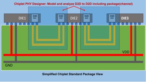
Keysight Technologies introduces the Chiplet PHY Designer, a novel electronic design automation (EDA) tool aimed at refining the verification process for die-to-die (D2D) interconnects. This tool is a pivotal addition to Keysight’s suite of high-speed digital design and simulation tools, concentrating on validating the performance of heterogeneous and 3D integrated circuit (IC) designs, commonly known as chiplets.
A standout feature of the Chiplet PHY Designer is its claim to be the industry’s first EDA tool with comprehensive modeling and simulation capabilities tailored to assist chiplet designers in ensuring their designs adhere to the specifications of the Universal Chiplet Interconnect Express (UCIe) standard. UCIe is gaining prominence as a chiplet interconnect specification in the semiconductor industry, defining interconnects within advanced 2.5D or 3D packages.
According to Niels Faché, Vice President and General Manager at Keysight EDA, the tool addresses critical interconnect performance issues, enhancing predictive virtual prototyping and expediting time-to-market for 3D IC designers. Faché stated, “The ‘Chiplet PHY Designer’ accelerates validation of chiplet subsystems, from one D2D PHY through interconnect channels to another D2D PHY, much earlier in the design cycle. It enables 3D IC designers to solve critical interconnect performance problems, improving predictive virtual prototyping to speed time-to-market.”
The tool supports the UCIe physical layer standard, facilitating automated parsing of signals according to standard naming conventions and enabling automated connections between multiple dies through package interconnects. The standardized simulation setup includes parameters such as speed grade, with an intuitive measurement setup through specialized probe components.
Adrien Auge, Senior Staff Applications Engineer at Alphawave Semi, emphasized the significance of validating chiplet solutions for enabling heterogeneous chip design. Auge expressed, “The ‘Chiplet PHY Designer’ simplifies the electrical simulation process for large die-die electrical connectivity, such as UCIe. It provides engineers and designers a quick and easy path to extract electrical compliance of their solutions against the latest revision of the specification.”
The UCIe standard is gaining traction within the semiconductor industry, with numerous top equipment vendors, EDA tool providers, foundries, and chiplet designers either supporting or adopting the standard. This open standard aims to establish a broad ecosystem for chiplet interoperability and commerce.


