
Fonon Corporation, a leading provider of laser material processing solutions, has introduced the BlackStar Wafer Dicing Machine, designed to address key challenges in the semiconductor industry.
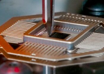
The BlackStar machine is powered by Fonon’s patented Fantom Width Laser Dicing (FWLD) technology, offering a novel approach to semiconductor wafer dicing. By utilizing FWLD, the machine can achieve precise molecular-level splitting with minimal kerf width, leading to reduced material waste and enhanced chip yield.
Semiconductor manufacturing often encounters issues such as defects, distortions, and material wastage during the dicing process. With conventional methods, such as silicon sawing tools, these challenges can lead to inefficiencies and increased production costs. However, Fonon’s BlackStar aims to mitigate these issues by ensuring the integrity of the material while maximizing throughput.
Through non-contact laser processing, the BlackStar minimizes flaking at the cut edge, thereby improving the quality of edges crucial for fracture resistance. Additionally, Fonon’s automated single-step processing further enhances chip reliability and quality, contributing to overall product dependability.
The versatility of Fonon’s FWLD technology enables the dicing of complex shapes and the production of multiple size dies on the same wafer. This flexibility not only fosters innovation in semiconductor design but also enhances manufacturing efficiency.
Moreover, the BlackStar’s compatibility with a wide range of semiconductor materials, including silicon, gallium arsenide, and silicon carbide, makes it a versatile solution for the industry.
In summary, Fonon’s BlackStar Wafer Dicing Machine represents a significant step forward in semiconductor manufacturing technology. With its innovative FWLD technology, it promises to reduce material waste and improve chip yield, thereby contributing to enhanced efficiency and cost-effectiveness in the semiconductor industry.