
In today’s interconnected world, Printed Circuit Boards (PCBs) serve as the backbone of modern electronic devices, facilitating seamless connectivity and powering technological advancements across various sectors. From their early beginnings to the present day, PCBs have undergone remarkable evolution, fueled by relentless innovation and the demand for higher performance and miniaturization. Join us as we embark on an exploration of the profound impact and latest breakthroughs in PCB technology.
Historical Milestones: Laying the Foundation for Modern PCBs
The journey of PCBs traces back to the early 20th century when pioneers in electronics experimented with different methods of creating electrical paths on insulating surfaces. German inventor Albert Hanson’s introduction of flat foil conductors in 1903 and Thomas Edison’s investigations into chemical plating on linen paper in 1904 laid the groundwork for the development of PCB technology.
Prominence and Advantages: Accelerating Efficiency and Cost-Effectiveness
Since American inventor Charles Ducas patented the “Printed wire” technique in 1925, PCBs have risen to prominence in the electronics industry. PCBs offer numerous advantages, making them the preferred choice for circuitry. Streamlined manufacturing processes through automated assembly enable efficient production, resulting in cost and time efficiencies. The high component density achievable with PCBs allows for intricate designs within limited space, while also improving signal integrity.
Technological Advancements: Pushing the Boundaries of Complexity and Functionality
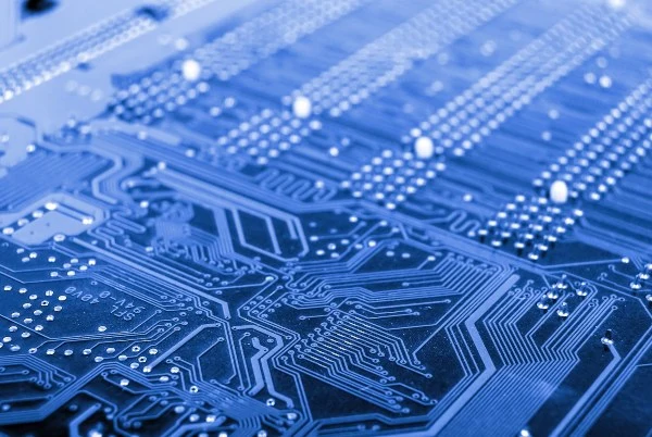
The advent of surface mount technology (SMT) and multilayer PCBs has ushered in a new era of electronic advancements. Multilayer PCBs, featuring multiple copper planes, allow for the integration of complex circuitry within a compact form factor. This breakthrough enables electronic devices to become more powerful and feature-rich. However, repairs and modifications pose challenges due to the intricate nature of multilayer PCBs.
Market Size and Growth: Expanding Horizons for PCB Applications
The global market for bare PCBs exceeded $60.2 billion in 2014, with projections estimating its value to reach $79 billion by 2024. This surge in demand is fueled by the rapid proliferation of electronic devices in sectors such as automotive, aerospace, telecommunications, consumer electronics, and healthcare. PCBs play a critical role in powering and connecting these devices, underscoring their significance in the ever-growing electronics industry.
Cutting-Edge Innovations: Exploring the Frontiers of PCB Technology
Flexible PCBs: The advent of flexible PCBs has revolutionized design possibilities, enabling the creation of curved or irregularly shaped electronic products. These flexible substrates offer increased versatility, reduced weight, and enhanced durability, finding applications in industries like automotive, wearable technology, and medical devices. Flexible PCBs provide designers with unprecedented freedom to create innovative and ergonomic designs.
High-Frequency PCBs: With the growing demand for faster data transmission, high-frequency PCBs have emerged as a vital component in advanced communication systems. These PCBs are designed with specialized materials and stringent impedance control to facilitate high-speed data transfer in industries such as telecommunications, aerospace, and defense. High-frequency PCBs enable the seamless flow of data, supporting the ever-increasing bandwidth requirements of modern communication networks.
Scientific Developments and Future Prospects: Transforming PCBs for Tomorrow
Continuous scientific research drives the evolution of PCBs, focusing on developing novel materials, advanced manufacturing techniques, and groundbreaking applications. Some notable advancements include:
3D Printing of PCBs: Researchers are exploring the potential of 3D printing techniques to fabricate intricate PCBs with integrated components. This approach enables rapid prototyping, customization, and on-demand manufacturing, opening doors to new design possibilities and reducing time-to-market. 3D-printed PCBs hold promise for faster prototyping cycles and the ability to create complex geometries and integrated electronic structures.
Internet of Things (IoT) Integration: PCBs are integral to the growth of IoT by connecting a multitude of devices and enabling data exchange. PCBs designed for IoT applications focus on power efficiency, compact form factors, and wireless connectivity. As the IoT ecosystem expands, PCB technology continues to evolve to meet the specific demands of this interconnected network.
Biodegradable PCBs: With a push towards sustainable business practices globally, there is an increasing focus on reducing e-waste by developing biodegradable materials for use in electronic products. Researchers are exploring environmentally friendly alternatives that maintain performance while minimizing the impact on the environment.
High-Density Interconnect (HDI) Technology: To meet the demand for faster signal transmission speeds and more compact interconnectivity between devices, High-Density Interconnect (HDI) technology has emerged. HDI technology enables the design and production of PCBs with higher component density, finer lines, and smaller vias, leading to improved performance and miniaturization.
As PCB technology continues to evolve, future prospects include advancements in materials science, manufacturing techniques, and integration with emerging technologies like artificial intelligence (AI) and quantum computing. PCBs are poised to play a pivotal role in shaping the next generation of electronic devices, paving the way for transformative innovations across industries.
The progressive journey of Printed Circuit Boards (PCBs) has transformed the electronics industry, powering the devices that define our modern world. From historical milestones to cutting-edge innovations, PCB technology continues to push boundaries and unlock new possibilities. As experts in the field, we are excited to witness the ongoing evolution of PCBs and the immense potential they hold for the future.