The Biden-Harris Administration announced that the U.S. Department of Commerce (DOC) is entering negotiations to invest up to $300 million in advanced packaging research projects in Georgia, California, and Arizona to accelerate the development of cutting-edge technologies essential to the semiconductor industry. The expected recipients are Absolics Inc. in Georgia, Applied Materials Inc. in California, and Arizona State University in Arizona.
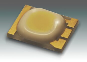
These competitively awarded research investments, each expected to total as much as $100 million, represent novel efforts in advanced substrates. Advanced substrates are physical platforms that allow multiple semiconductor chips to be assembled seamlessly together, enable high-bandwidth communication between those chips, efficiently deliver power, and dissipate unwanted heat. The advanced packaging enabled by advanced substrates translates to high performance computing for AI, next-generation wireless communication, and more efficient power electronics. Such substrates are not currently produced in the United States but are foundational to establishing and expanding domestic advanced packaging capability. Up to $300 million in federal funding will be paired with additional investments from the private sector, bringing the expected total investment across all three projects to over $470 million. This combined effort will help ensure U.S. manufacturers stay competitive and continue to drive technological innovation, giving companies a stronger edge in global competition.
“The key to the United States’ long-term competitiveness hinges on our ability to out-innovate and out-build the rest of the world. That’s why the R&D side of the CHIPS for America Program is so fundamental to our success, and these proposed investments in advanced packaging underscore the work we’re doing to prioritize every step of the semiconductor supply chain pipeline,” said U.S. Secretary of Commerce Gina Raimondo. “Emerging technology like AI requires cutting-edge advances in microelectronics, including advanced packaging. Thanks to President Biden’s and Vice President Harris’ leadership, and through these proposed investments, we are positioning the United States as a global leader in designing, manufacturing and packaging the microelectronics that will fuel tomorrow’s innovation.”
“Today’s awards are vital to secure America’s global leadership in semiconductors– making sure the supply chain here in America is on the cutting edge from end to end,” said National Economic Advisor Lael Brainard.
Rising power consumption, computational performance in AI data centers, and scalability in mobile electronics will not be solved with current packaging technology. Sustaining these industries of the future in America will require innovation at all levels. The CHIPS National Advanced Packaging Manufacturing Program (NAPMP) set aggressive technical targets for the substrates that all three entities are expected to meet or exceed. Advanced substrates are the basis for advanced packaging, which will enhance key advanced packaging technologies including but not limited to equipment, tools, processes, and process integration. The projects will play a vital role in helping to ensure that American innovation drives cutting-edge developments in semiconductor research and development (R&D) and manufacturing.
“Advanced packaging is essential to the development of the advanced semiconductors that are the drivers of emerging technology like artificial intelligence,” said Under Secretary of Commerce for Standards and Technology and National Institute of Standards and Technology Director Laurie E. Locascio. “These first investments of the National Advanced Packaging Manufacturing Program will drive breakthroughs that address a critical need in the CHIPS for America’s mission to create a robust domestic packaging industry where advanced node chips manufactured in the U.S. and abroad can be packaged within the United States.”
The proposed projects are:
- Absolics, Inc. in Covington, Georgia: Absolics is poised to revolutionize glass core substrate panel manufacturing by developing cutting-edge capabilities in partnership with over 30 partners including academic institutions, large and small businesses, and non-profit entities, having been recognized as the recipient in the glass materials and substrates areas, with up to $100 million in potential funding. Through its Substrate and Materials Advanced Research and Technology (SMART) Packaging Program, Absolics aims to build a glass-core packaging ecosystem. In addition to developing the SMART Packaging Program, Absolics and their partners, is planning to support education and workforce development efforts by bringing training, internship, and certification opportunities into technical colleges, the HBCU CHIPS Network, and Veterans programs. Through these efforts, Absolics would leapfrog the current glass core substrate panel technology and support investments in a future high-volume manufacturing capability.
- Applied Materials in Santa Clara, California: Applied Materials, along with a team of 10 collaborators, is working on developing and scaling a disruptive silicon-core substrate technology for next-generation advanced packaging and 3D heterogeneous integration. Applied’s silicon-core substrate technology has the potential to advance America’s leadership in advanced packaging and help catalyze an ecosystem to develop and build next-generation energy-efficient artificial intelligence (AI) and high-performance computing (HPC) systems in the US. In addition, Applied Materials’ education and workforce development plan is designed to strengthen the training and internship pipeline in the US between state universities and the semiconductor industry.
- Arizona State University in Tempe, Arizona: Arizona State University is leading the charge in developing the next generation of microelectronics packaging through fan-out-wafer-level-processing (FOWLP). At the heart of this initiative is the ASU Advanced Electronics and Photonics Core Facility, where researchers are exploring the commercial viability of 300 mm wafer-level and 600 mm panel-level manufacturing, a technology that does not exist in as a commercial capability in the U.S. today. ASU’s team of over 10 partners, led by industry pioneer Deca Technologies, is centered in a regional stronghold for microelectronics manufacturing and is composed of large and small businesses, universities and technical colleges, and non-profits. This team spans the entire United States with industrial leaders in materials, equipment, chiplet design, electronic design automation, and manufacturing. ASU will establish an interconnect foundry that connects advanced packaging and workforce development programs with semiconductor fabs and manufacturers. ASU’s education and workforce development efforts bring industry-relevant training such as train the trainer, microcredentials, and quick start programs for working professionals. Inclusion of the HBCU CHIPS network and the National Center for American Indian Enterprise Development is integral to their workforce development plan.
(Source: Chip.Gov)


