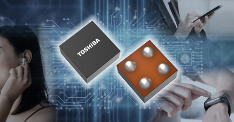
Toshiba Electronic Devices & Storage Corporation has brought to market the “TCK12xBG Series” of load switch ICs that deliver a remarkable decrease in quiescent current and an output current rating of 1A. Housed in a small WCSP4G package, the new ICs will support product developers in innovating a new generation of wearables and IoT devices that consume less power and offer a longer charge life. Volume shipments start today.
TCK12xBG Series uses a new driver circuit, which realizes a typical ON-state quiescent current of 0.08nA. This represents in the region of 99.9% reduction from Toshiba’s current product, “TCK107AG,” a huge advance in efficiency that will allow wearables and IoT devices powered by small batteries to operate for significantly longer.
WCSP4G, a new package developed for the products, is about 34% smaller than that of TCK107AG, only 0.645×0.645mm, which allows mounting on small boards. Its back coating can reduce the damage that can happen to such a minute chip in the mounting process.
Toshiba has prepared a line-up of three ICs: TCK127BG with automatic discharge that turns on at active high; TCK126BG without automatic discharge that turns on at active high; and TCK128BG with automatic discharge that turns on at active low. This offers product developers and designers the freedom to select the load switch IC that best suits their design requirement.
Toshiba will continue to enhance low quiescent current technology products, to contribute to equipment downsizing and lower power consumption, and to a sustainable future.
Applications
- Wearables, IoT devices, smartphones (ON and OFF switch of power supply for sensors, etc.)
- Replacement of load switch circuits formed by discrete semiconductors such as MOSFETs, transistors, etc.
Features
- Ultra-low quiescent current (ON state): IQ=0.08nA (typ.)
- Low standby current (OFF state): IQ(OFF)+ISD(OFF)=13nA (typ.)
- Compact WCSP4G package: 0.645×0.645mm (typ.), t:0.465mm (max.)
- Backside coating that reduces damage in board-mounting process


