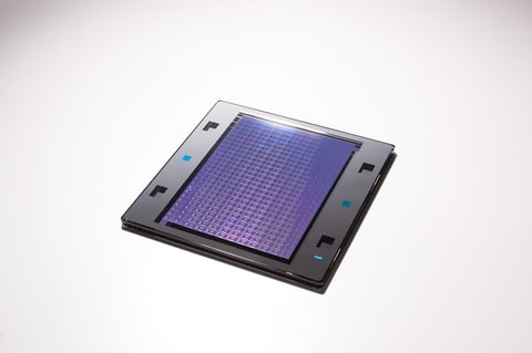
Dai Nippon Printing Co., Ltd. (DNP, TOKYO: 7912) has successfully achieved the fine pattern resolution required for photomasks for logic semiconductors of the beyond 2nm (nm: 10-9 meter) generation1 that support Extreme Ultra-Violet (EUV) lithography, a cutting-edge process in semiconductor manufacturing.
DNP has also completed the criteria evaluation for photomasks compatible with High-Numerical Aperture2, the application being considered for next-generation semiconductors beyond the 2nm generation, and has commenced the supply of evaluation photomasks. High-NA EUV lithography makes it possible to form fine patterns on silicon wafers with a higher resolution than previously possible, and is expected to lead to the realization of high-performance, low-power semiconductors.
This will help in the development of photomasks for beyond 2nm generation extreme ultraviolet (EUV) lithography. To meet the stringent requirements of next-generation semiconductor manufacturing, DNP has successfully achieved the pattern resolution needed for beyond 2nm generation through iterative enhancements of its established 3nm generation manufacturing processes.
The breakthrough addresses the challenge of producing patterns that are 20% smaller than those used in the 3nm generation, while accommodating increasingly complex curved and fine patterns. This advancement is crucial as the industry shifts towards high numerical aperture (NA) EUV lithography, which demands higher precision and finer processing compared to standard EUV lithography. DNP has developed and optimized an entirely new manufacturing process flow to meet these requirements.
Looking ahead, DNP plans to commence mass production of photomasks for 2nm generation logic semiconductors by FY 2027. The company is also collaborating with imec, a global leader in nanoelectronics research, to accelerate the development of photomask technologies with an eye on the 1nm generation, solidifying its position at the forefront of semiconductor innovation.


